Gate-tunable heterojunction tunnel triodes based on 2D metal selenide and 3D silicon
Electronics engineers worldwide are trying to improve the performance of devices, while also lowering their power consumption. Tunnel field-effect transistors (TFETs), an experimental class of transistors with a unique switching mechanism, could be a particularly promising solution for developing low-power electronics.

Despite their potential, most TFETs based on silicon and III-V heterojunctions exhibit low on-current densities and on/off current ratios in some modes of operation. Fabricating these transistors using 2D materials could help to improve electrostatic control, potentially increasing their on-current densities and on/off ratios.
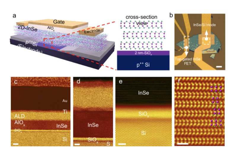
Researchers at University of Pennsylvania, the Chinese Academy of Sciences, the National Institute of Standards and Technology, and the Air Force Research Laboratory have recently developed new heterojunction tunnel triodes based on van der Waals heterostructures formed from 2D metal selenide and 3D silicon. These triodes, presented in a paper published in Nature Electronics, could outperform other TFETs presented in the past in terms of on-current densities and on/off ratios.
"This paper is based on the realization of tunneling transistors or switching devices based on 2D materials," Deep Jariwala, one of the researchers who carried out the study, told TechXplore. "It is a well-known idea that many people have been trying to work on and solve for a decade now. The issue has always been performance of the devices to make a strong case."
To improve the performance of tunneling switching devices in terms of ON/OFF current ratios, subthreshold swing and ON current density, some studies tried to develop devices using solely silicon and III-V semiconductors or 2D semiconductors. While some of these proposed devices performed better than others, their performance appeared to be impaired in at least one relevant dimension.
"With our work, we have shown that when 2D InSe or WSe2 is combined with silicon all three major performance characteristics of the device mentioned above can be simultaneously improved," Jariwala explained.
To fabricate their heterojunction tunnel triodes, Jariwala and his colleagues stamped an InSe crystal onto a heavily p-doped silicon wafer. Subsequently, they created contacts using lithography, a printing method, deposited a top gate-dielectric, and patterned gate electrodes.
"One key advantage of our gate-tunable tunnel triodes is that they are based on silicon, which is the underlying material for all microprocessors," Jariwala said. "In addition, they have some of the steepest sub-threshold swings, ON/OFF current ratios and On current density for tunneling devices, making them some of the most energy efficient and effective switches based on tunneling phenomena."
In initial tests, the triodes created by the researchers attained subthreshold slopes as low as 6.4 mV decade-1 and average subthreshold slopes of 34.0 mV decade-1 over four decades of drain current. Remarkably, they also exhibited a current on/off ratio of approximately 106 and an on-state current density of 0.3 µA µm–1 at a drain bias of –1 V.
"We showed that InSe works as an excellent 2D semiconductor in combination with good old silicon for enabling some of the most energy efficient switching devices," Jariwala said. "The possible implications of this finding are immense, since energy efficiency (and not Moore's law for scaling down devices) is the key requirement/need of the hour in terms of innovation at the device level in microelectronics."
The heterojunction tunnel triodes introduced by Jariwala and his colleagues could pave the way towards the realization of better performing low-power electronic devices. In principle, their design could also be scaled up to wafers, given that InSe-based 2D materials can be directly grown on silicon.
"In our next studies, we plan to scale up the material growth to make it more practical and scale down the device dimensions to improve the performance even further," Jariwala added. "Demonstrating the material growth over a large area on a wafer will be a big milestone which we hope to achieve by next year."


